Our engineers work with a lot of Gerber files. You probably know what that means, but just in case you don’t, Gerber is the file format for submitting printed circuit board (PCB) file designs to a PCB manufacturer. When you’re developing a product that includes electronics, you will have to supply Gerber files along with all your other product design files.
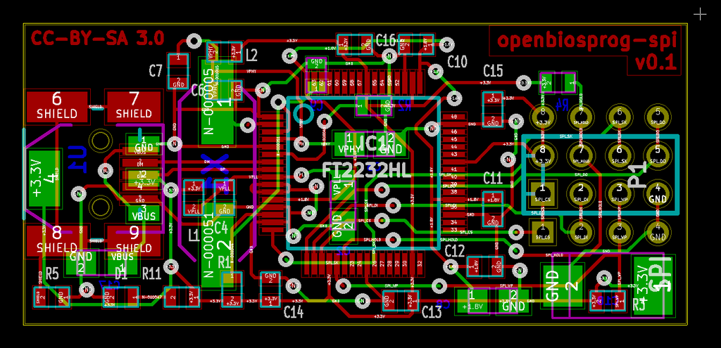
We recently asked our Senior Product Development Engineer, Agustin Guzman, the most common problems he saw when he got Gerber files. The following four problems came off the top of his head without much thought, and the solution for each was the same: pay attention to the manufacturer’s data sheets.
If you're like me - not an engineer - and you're dying to see what a data sheet looks like, here is a very simple data sheet for a SMD 6mm square SPST button made by Sparkfun.
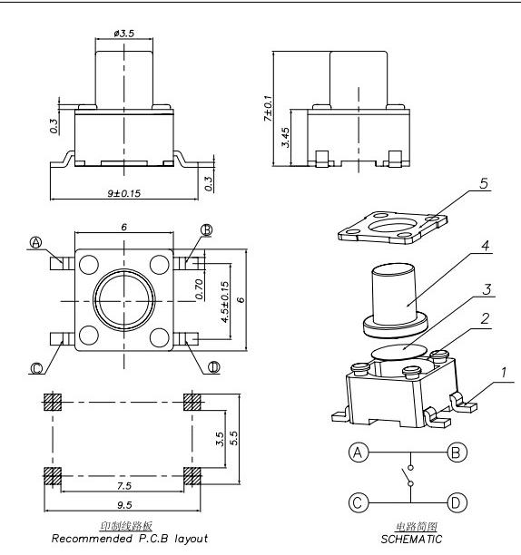
Image courtesy of Sparkfun/CC
So, you're wondering, what's wrong with my Gerber files?
PROBLEM 1
The files call for the wrong hole size on through hole components and wrong pad size on surface mount components. For example, you might have a customer use a component with leads that are 1 mm in diameter on a hole that is also 1 mm in diameter. That’s not going to work because of variability in manufacturing.
Solution?
Read the data sheet that comes with the component. Every component comes with a data sheet supplied by the manufacturer. Data sheets are a map of how the component is built and then placed on the circuit board.
In the case of the wrong size hole or pad, follow the data sheet directions to the letter. You need to drill a hole to the exact spec and use the exact pad size.
PROBLEM 2
The components are laid out too close or holes are cut too close. That often means the components can’t physically be placed on the board. The clearances are reeeeeeallly tight around the components for the pick and place machines to operate.
.jpg?width=2189&height=2349&name=Gerber-2-East-West-MFG%20(2).jpg)
Solution?
Pay attention to the actual size of the component and what's around it. Again, the manufacturers data sheet is your best guide.
PROBLEM 3
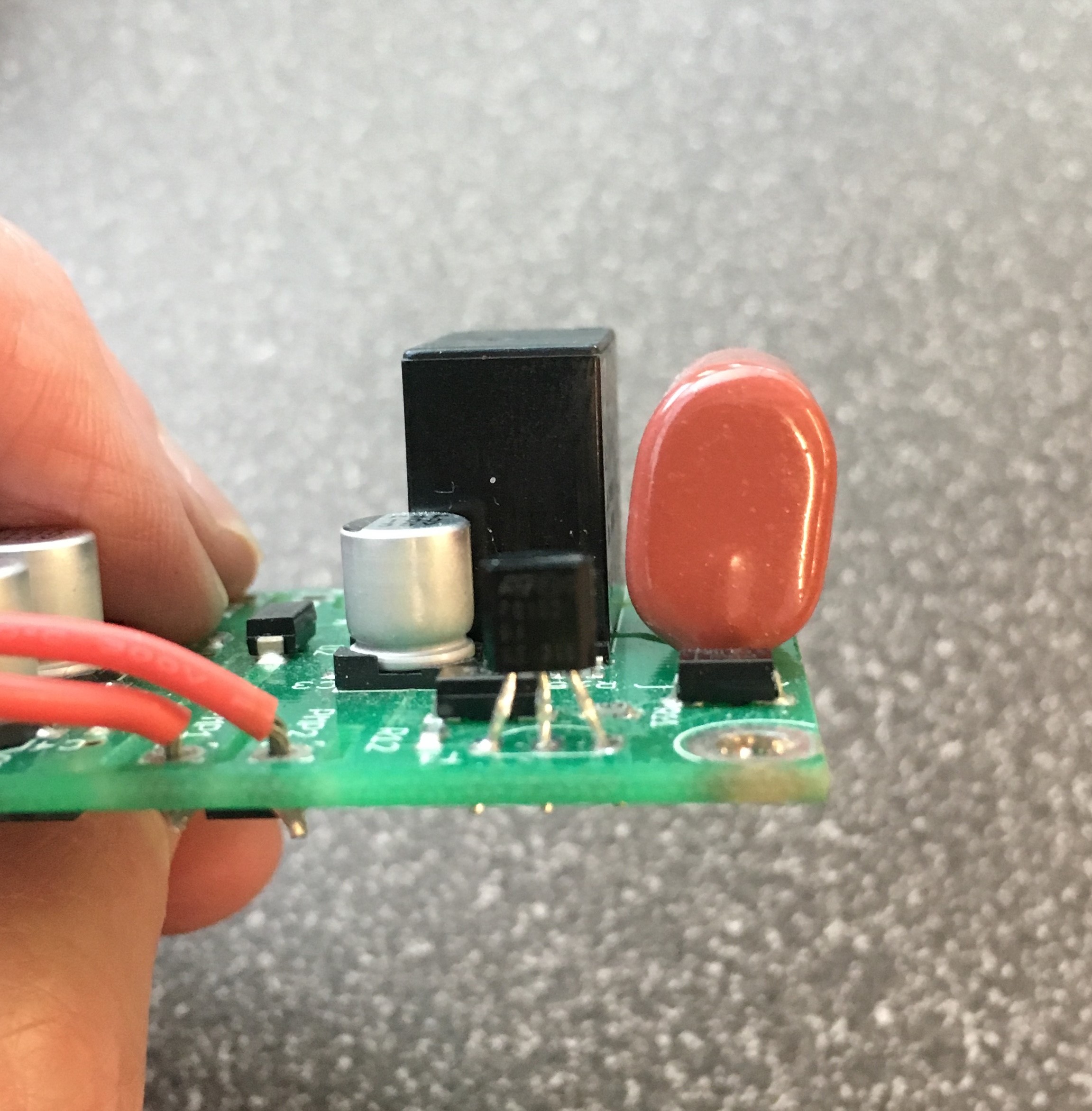
The components are large and hang off the PCB. See the reddish component below? It hangs just a little bit over to the side. You'd be surprised by just how much of a problem that little bit of overhang can cause.
Solution?
Have we mentioned the manufacturer’s data sheets? Sometimes people think, well the holes are on the board so that means the components will fit on the board. Not necessarily. The component might be soldered onto the board but its case could hang off, even a little bit can cause problems if the enclosed part won't fit around the component. Pay attention to the physical dimensions of the component. Read the data sheet.
PROBLEM 4
The routed slots are too close to pads or traces.
Solution?
Review all tolerances and parts fitment in a PCB layout software.
It often seems like the simplest solution is the one right in front of you. In this case it really is true. The manufacturer's data sheets provide all the information you need to put together a good set of Gerber files. In fact, for the most accurate Gerbers, ask the manufacturer if they have a downloadable component library (which will include a component footprint). That means you download the component library and place it right on your schematic and PCB.
What could be easier?
Read more:


.jpg?width=176&height=56&name=MR_associatedNetwork_logo%20(1).jpg)